WCR03-12WM
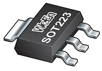
Planar passivated SCR with sensitive gate in surface mountable plastic package and through-hole package. This SCR is designed to be interfaced directly to microcontrollers, logic integrated circuits and other low power gate trigger circuits.
Features and Benefits
- On-state RMS current, 1.25 A
- Repetitive peak off-state voltage, 1250 V
- High surge current capability
- Direct triggering from low power drivers and logic ICs
- Planar passivated for voltage ruggedness and reliability
- Through-hole package (TO92)
Applications
- GFCI (Ground Fault Circuit Interrupter)
- AFCI (Arc Fault Circuit Interrupter)
- RCD (Residual Current Device)
- RCBO (Residual Current circuit Breaker with Overload protection)
- AFDD (Arc Fault Detection Device)
| Type Number | Symbol | Parameter | Conditions | Min | Typ/Nom | Max | Unit |
| WCR03-12WM | VDRM | repetitive peak off-state voltage | 1250 | V | |||
| VRRM | repetitive peak reverse voltage | 1250 | V | ||||
| IT(AV) | average on-state current | half sine wave; Tc ≤ 110 °C | 0.8 | A | |||
| IT(RMS) | RMS on-state current | half sine wave; Tc ≤ 110 °C | 1.25 | A | |||
| ITSM | non-repetitive peak on-state current |
half sine wave; Tj(init) = 25 °C; tp = 10 ms | 20 | A | |||
| half sine wave; Tj(init) = 25 °C; tp = 8.3 ms | 22 | A | |||||
| Tj | junction temperature | 125 | °C | ||||
| IGT | gate trigger current | VD = 12 V; RL = 100 Ω; Tj = 25 °C | 10 | 90 | μA | ||
| IL | latching current | IT = 0.1 A; RGK = 1 kΩ; Tj = 25 °C | 6 | mA | |||
| IH | holding current | VD = 12 V; RGK = 1 kΩ; Tj = 25 °C | 5 | mA | |||
| dVD/dt | rate of rise of off-state voltage | VDM = 838 V; Tj = 125 °C; RGK = 1 kΩ ; (VDM = 67% of VDRM); exponential waveform |
200 | V/µs |


