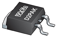
ACTT10B-800CTN
AC Thyristor Triac power switch in a TO263 (D2PAK) surface mountable plastic package with self-protective clamping capabilities against low and high energy transients. This "series CTN" triac will commutate the full RMS current at the maximum rated junction temperature (Tj(max) = 150 °C) without the aid of a snubber. It is used in applications where "high junction operating temperature capability" is required.
Features and Benefits
• Clamping structure ensuring safe high over-voltage withstand capability
• High junction operating temperature capability (Tj(max) = 150 °C)
• High minimum IGT for guaranteed immunity to gate noise
• Full cycle AC conduction
• Over-voltage withstand capability to IEC 61000-4-5
• Pin compatible with standard triacs
• Planar passivated for voltage ruggedness and reliability
• Protective self turn-on capability for high energy transients
• Safe clamping capability for low energy over-voltage transients
• Less sensitive gate for high noise immunity
• Surface mountable package
• Triggering in three quadrants only
• Very high immunity to false turn-on by dV/dt and IEC 61000-4-4 fast transient
• Package meets UL94V0 flammability requirement
• Package is RoHS compliant
Applications
• AC fan, pump and compressor controls
• Highly inductive, resistive and safety loads
• Large and small appliances (White Goods)
• Reversing induction motor controls
• Applications subject to high temperature (Tj(max) = 150 °C)
| Type Number | Symbol | Parameter | Conditions | Min | Typ/Nom | Max | Unit |
|---|---|---|---|---|---|---|---|
| ACTT10B-800CTN | VDRM | 800 | V | ||||
| IT(RMS) | RMS on-state current | square-wave pulse; Tmb ≤ 126 °C; Fig. 1; Fig. 2; Fig. 3 | 10 | A | |||
| ITSM | non-repetitive peak on-state current | full sine wave; tp = 20 ms; Tj(init) = 25 °C; Fig. 4; Fig. 5 | 90 | ||||
| non-repetitive peak forward current | full sine wave; tp = 16.7 ms; Tj(init) = 25 °C; | 99 | |||||
| Tj | junction temperature | 150 | °C | ||||
| IGT | gate trigger current | VD = 12 V; IT = 0.1 A; T2+ G+ Tj = 25 °C; Fig. 7 | 5 | 35 | mA | ||
| VD = 12 V; IT = 0.1 A; T2+ GTj = 25 °C; Fig. 7 | 5 | 35 | mA | ||||
| VD = 12 V; IT = 0.1 A; T2- GTj = 25 °C; Fig. 7 | 5 | 35 | mA | ||||
| IH | holding current | VD = 12 V; Tj = 25 °C; Fig. 9 | 30 | mA | |||
| Vt | on-state voltage | IT = 14 A; Tj = 25 °C; Fig. 10 | 1.5 | V | |||
| dVD/dt | rate of rise of off-state voltage | VDM = 536 V; Tj = 150 °C; (VDM = 67% of VDRM); exponential waveform; gate open circuit | 2000 | V/μs | |||
| dIcom/dt | rate of change of commutating current | VD = 400 V; Tj = 150 °C; IT(RMS) = 10 A; dVcom/dt = 20 V/μs; gate open circuit; snubberless condition | 5 | A/ms |


