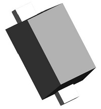
ESDHD05BB

The ESDHDxxBB series are designed to protect voltage sensitive components which are connected to data and transmission lines from overvoltage caused by ESD (electrostatic discharge), CDE (Cable Discharge Events), and EFT (electrical fast transients). Excellent clamping capability, low leakage, and fast response time, make these parts ideal for ESD protection on designs where board space is at a premium.

Features and Benefits
  • Transient protection for high-speed data lines
  • Peak pulse power 90W @ 8/20μs waveform
  • IEC 61000-4-2 (ESD) ±30kV(air), ±30kV(contact)
  • Protects Bi-directional I/O line
  • Low clamping voltage
  • Low leakage current
  • Meet MSL level1
  • Halogen free and RoHS compliant
Applications
  • Computer Interfaces Protection
  • Microprocessors Protection
  • Serial and Parallel Ports Protection
  • Control Signal Lines Protection
  • Power lines on PCB Protection
  • Portable instrumentation
  • Peripherals
Parametric
Package
Quality, reliability & chemical content
Ordering
Type Number Symbol Parameter Conditions Min Typ/Nom Max Unit
   ESDHD05BB VR  reverse working voltage       5 V
VBR  reverse breakdown voltage  IT = 1 mA 5.6     V
Tj  junction temperature   -55   150 °C
VC  clamping voltage  IPP = 1 A; tp = 8/20 μs     8.5 V
 IPP = 9 A; tp = 8/20 μs     10 V
IPP  peak pulse current  8/20μs waveform     9 A
IR  reverse leakage current  VR = 5 V     1 μA
Cj  Junction Capacitance  VR = 0 V; f = 1 MHz;   15   pF
Type number Package Packing Product status Marking Orderable part number Ordering code (12NC)
ESDHD05BB

SOD523

STANDARD MARK SMD Volume production Standard Marking ESDHD05BBX 9340 730 03115
Datasheet
Type number Ordering code (12NC) Orderable part number Region Distributor Order sample
ESDHD05BB 9340 730 03115 ESDHD05BBX NA NA  

Please login or register before apply WeEn sample.

Image CAPTCHA
Chemical content Orderable part number Type number RoHS / RHF Leadfree conversion date MSL MSL LF
ESDHD05BB ESDHD05BBX ESDHD05BB Leaded  H      

Disclaimer

All information in this document is furnished for exploratory or indicative purposes only. All information in this document is believed to be accurate and reliable. However, WeEn Semiconductors does not give any representations or warranties as to the accuracy or completeness of such information and shall have no liability for the consequences of use of such information. WeEn Semiconductors may make changes to information published in this document at any time and without notice. Minor deviations may occur in the products from different manufacturing location. This document supersedes and replaces all information supplied prior to the publication hereof. Nothing in this document may be interpreted or construed as an offer to sell products that is open for acceptance or the grant, conveyance or implication of any license under any copyrights, patents or other industrial or intellectual property rights.